

In the relentless pursuit of faster, more efficient computing, 3D chip stacking has emerged as a revolutionary breakthrough, fundamentally transforming how we design and build semiconductor devices. By vertically integrating multiple layers of silicon chips, this technology shatters the traditional two-dimensional limitations that have constrained processor development for decades. Think of it as building a high-rise apartment complex instead of spreading houses across a suburb – it dramatically increases processing power while minimizing the physical footprint.
As artificial intelligence and machine learning demands push computing requirements to unprecedented levels, 3D chip stacking offers a compelling solution. This architectural approach not only packs more transistors into a given area but also significantly reduces the distance signals need to travel, leading to faster processing speeds and lower power consumption. Industry giants like Intel, TSMC, and Samsung are already leveraging this technology to create next-generation chips that promise to accelerate AI workloads while addressing the growing concerns about energy efficiency in data centers.
This transformative technology represents more than just an incremental improvement – it’s a paradigm shift in semiconductor design that could help sustain Moore’s Law well into the future.
How 3D Chip Stacking Revolutionizes AI Hardware
Traditional vs. 3D Architecture
In the world of semiconductor design, traditional chip architectures have relied on a flat, two-dimensional layout where components are arranged side by side. This planar approach has served the industry well for decades but is reaching its physical limits as we push for more computing power in smaller spaces.
3D chip stacking represents a paradigm shift by building vertically instead of horizontally. Imagine transforming a sprawling single-story building into a sleek skyscraper – that’s essentially what happens when we stack chip components in three dimensions. This vertical arrangement allows for shorter interconnects between different parts of the chip, reducing signal travel distance and power consumption.
The traditional planar design requires signals to travel longer distances across the chip’s surface, leading to increased latency and power usage. In contrast, 3D stacking creates direct vertical pathways between components, similar to having an elevator in a building instead of walking around the block. This architectural evolution has become particularly crucial for AI applications, where processing speed and energy efficiency directly impact performance.

The Physics Behind Vertical Integration
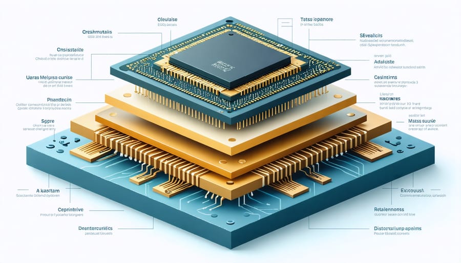
At its core, 3D chip stacking involves layering multiple silicon wafers vertically and connecting them using tiny through-silicon vias (TSVs). These TSVs are microscopic channels filled with conductive material, typically copper, that enable electrical signals to flow between the different layers. Think of it like a multi-story building where elevators (TSVs) connect different floors (chip layers).
The physics behind this integration relies on several key principles. First, the silicon wafers must be precisely thinned to reduce the overall package height and improve heat dissipation. This thinning process typically brings each layer down to about 50 micrometers – thinner than a human hair.
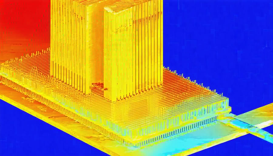
Heat management is crucial in 3D stacking. As electrical current flows through the TSVs and between layers, it generates heat that must be efficiently dispersed. Engineers use advanced thermal management techniques, including the strategic placement of thermal vias and incorporating specialized cooling layers.
The vertical arrangement significantly reduces the distance signals need to travel between components, leading to faster processing speeds and lower power consumption compared to traditional 2D layouts.
AI-Specific Benefits of 3D Chip Stacking
Faster Memory Access for Neural Networks
One of the most significant advantages of 3D chip stacking in AI applications is its ability to drastically reduce memory access times. Traditional 2D chip designs often struggle with the “memory wall” – the growing gap between processor and memory speeds. By vertically stacking memory layers directly above processing elements, memory architectures for AI training can achieve significantly faster data transfer rates.
This vertical integration creates shorter electrical pathways between memory and processing units, reducing latency and power consumption. Instead of data traveling horizontally across a motherboard through various interconnects, it now moves vertically through microscopic connections called through-silicon vias (TSVs). These TSVs can transfer data up to 1000 times faster than traditional horizontal connections.
For neural networks, which constantly need to access vast amounts of weights and activation values, this architectural improvement translates to remarkable performance gains. Training times can be reduced by up to 70% in some cases, while inference operations become nearly instantaneous. The shorter distances also mean less energy is wasted on moving data, making 3D-stacked chips more energy-efficient than their 2D counterparts.
This advancement is particularly crucial for edge AI devices, where quick memory access can mean the difference between real-time processing and noticeable delays in applications like autonomous vehicles or augmented reality systems.
Power Efficiency Improvements
One of the most compelling advantages of 3D chip stacking is its significant impact on power efficiency. By reducing the distance that signals need to travel between different components, this technology dramatically cuts down on energy consumption. Traditional 2D designs require signals to traverse longer paths, resulting in higher power usage and increased latency. In contrast, the vertical integration in 3D stacking can reduce these distances by up to 1000 times, leading to substantial energy savings.
The improved thermal management capabilities of 3D stacked chips also contribute to their power efficiency. Modern designs incorporate specialized cooling layers and thermal interface materials between the stacked dies, allowing for better heat dissipation. This enhanced thermal management means the chips can operate at optimal temperatures without requiring excessive cooling, further reducing overall power consumption.
Another key benefit is the ability to optimize different layers for specific power requirements. Engineers can design power-hungry processing layers with advanced power delivery networks while keeping memory layers more energy-efficient. This targeted approach to power management results in better overall system efficiency. Some implementations have shown power savings of up to 50% compared to traditional 2D designs, making 3D chip stacking particularly attractive for data centers and mobile devices where energy efficiency is crucial.
Current Implementation Challenges
Heat Management Solutions
As chip layers stack up, managing heat becomes increasingly critical. Modern 3D chip designs employ several innovative cooling solutions to prevent thermal issues from compromising performance. Liquid cooling systems, which circulate coolant through microscopic channels between chip layers, have emerged as a leading solution. These channels, often thinner than a human hair, efficiently draw heat away from critical components.
Advanced thermal interface materials (TIMs) play a crucial role by filling microscopic gaps between layers, ensuring optimal heat transfer. Some manufacturers are experimenting with diamond-based TIMs, which offer superior thermal conductivity compared to traditional materials.
Through-silicon vias (TSVs) serve a dual purpose: while primarily used for electrical connections, they also act as thermal conduits, helping dissipate heat vertically through the stack. Some designs incorporate dedicated thermal TSVs specifically for heat management.
Dynamic thermal management systems actively monitor temperatures across different layers and adjust processing loads accordingly, preventing hotspots from forming. When combined with AI-powered predictive cooling algorithms, these systems can anticipate and prevent thermal issues before they impact performance.
Manufacturing Complexity
Manufacturing 3D chip stacks presents significant engineering challenges that manufacturers must carefully navigate. The primary challenge lies in the precise alignment of multiple silicon layers, where even microscopic misalignments can render entire chips unusable. Heat management becomes increasingly complex as more layers are added, requiring innovative cooling solutions and thermal design considerations.
The manufacturing process also demands extremely clean environments, as any contamination between layers can create defects that compromise the chip’s functionality. Through-Silicon Vias (TSVs), the vertical connections between layers, must be created with exceptional precision, often requiring specialized equipment and processes.
However, manufacturers are developing promising solutions to address these challenges. Advanced alignment systems using machine learning algorithms help achieve precise layer positioning, while new cooling technologies like microfluidic channels between layers manage heat more effectively. Improved bonding techniques and quality control methods have also increased manufacturing yields significantly.
Recent innovations in automated inspection systems and real-time process monitoring have further enhanced production reliability, making 3D chip stacking increasingly viable for mass production despite its complexity.
Real-World Applications and Future Prospects
Success Stories in AI Acceleration
Several leading tech companies have demonstrated remarkable success with 3D chip stacking in AI applications. Apple’s M1 Ultra processor showcases the potential of this technology, using die-to-die interconnect to combine two M1 Max chips into a single powerful unit, dramatically improving AI task performance. This implementation has enabled up to 2.5x faster machine learning model training compared to traditional 2D designs.
NVIDIA’s A100 GPU, featuring 3D chip stacking technology, has become a cornerstone for many specialized AI computing solutions. The company reported up to 20x performance improvements in deep learning inference tasks, while reducing power consumption by 30% compared to previous architectures.
IBM’s latest AI accelerators demonstrate another compelling case study, where 3D stacking allowed for the integration of high-bandwidth memory directly with processing elements. This resulted in a 3x reduction in latency for large language model processing and a 40% smaller physical footprint compared to conventional designs.
These implementations showcase how 3D chip stacking is revolutionizing AI hardware, making advanced computing more efficient and accessible while addressing critical power and space constraints.
Next-Generation Developments
The future of 3D chip stacking is poised for revolutionary breakthroughs. Researchers are exploring innovative materials and architectures that could enable chips with hundreds of layers, dramatically surpassing current capabilities. One particularly promising development is the integration of optical interconnects, which could eliminate bottlenecks in data transfer between layers while significantly reducing power consumption.
Industry leaders are also investigating advanced cooling solutions, including microfluidic channels embedded within the chip layers, to address thermal management challenges. These developments are crucial for enabling more complex brain-like hardware processing systems that require dense interconnections and high computational power.
Emerging technologies like carbon nanotubes and graphene-based materials are being tested as alternatives to traditional silicon, potentially offering better thermal conductivity and electrical performance. Additionally, AI-assisted design tools are becoming instrumental in optimizing the complex layouts and interconnections required for next-generation 3D-stacked chips, promising more efficient and powerful computing solutions in the coming years.
As we look toward the future of AI computing, 3D chip stacking stands as a transformative technology that’s reshaping the landscape of artificial intelligence hardware. This innovative approach to chip design has already demonstrated its potential to dramatically improve AI processing capabilities while addressing critical challenges of power consumption and computational density.
The impact of 3D chip stacking on AI development cannot be overstated. By enabling faster data transfer, reduced latency, and improved energy efficiency, this technology is making it possible to create more powerful AI systems that can handle increasingly complex tasks. From autonomous vehicles to advanced natural language processing, the applications benefiting from 3D-stacked chips continue to expand.
Looking ahead, we can expect to see even more revolutionary developments in this field. Researchers are exploring new materials and manufacturing techniques that could push the boundaries of what’s possible with 3D chip stacking. The integration of novel cooling solutions and advanced packaging technologies promises to overcome current limitations and unlock even greater performance gains.
As AI continues to evolve and demand more computational power, 3D chip stacking will play a crucial role in meeting these requirements. This technology isn’t just an incremental improvement – it’s a fundamental shift in how we approach AI hardware design. For students, professionals, and organizations working in AI, understanding and leveraging 3D chip stacking will be essential for staying at the forefront of technological innovation.